The world's most complex machine (22 minute read)
ASML, a Dutch company, became the sole supplier of machines that make advanced semiconductors by betting on extreme ultraviolet lithography and embracing partnerships over vertical integration.
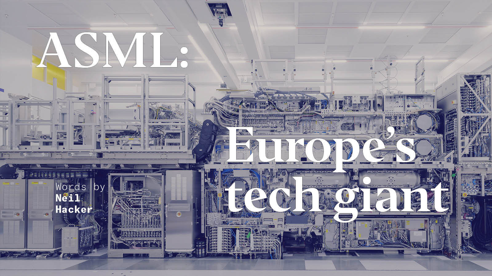
What: ASML manufactures the only photolithography machines capable of producing cutting-edge semiconductors with features as small as three nanometers. These bus-sized machines use extreme ultraviolet light to etch billions of transistors onto silicon wafers, selling for over $120 million each.
Why it matters: ASML's rise challenges conventional wisdom about how tech companies should operate. While Japanese rivals Nikon and Canon pursued vertical integration and secrecy, ASML succeeded through outsourcing, modular design, public-private partnerships with the US government, selling stakes to customers, and close collaboration with chipmakers like TSMC. This European success story depended entirely on transatlantic cooperation rather than going it alone.
Deep dive
- ASML started as a failing Philips spin-off in 1984 with just 20% market share, mocked for outsourcing components instead of vertical integration, and nearly shut down by 1988
- The company's modular design became an advantage because machines could be repaired on-site with swappable parts, reducing downtime compared to Japanese competitors
- ASML joined the US government's Extreme Ultraviolet LLC in 1997 after initially being barred as a foreign company, gaining access to $270M in research and full IP ownership when it acquired Silicon Valley Group in 2001
- Japanese rivals Nikon and Canon were never allowed into the consortium due to fears of Japanese competition, giving ASML a decisive advantage
- The Belgium-based IMEC research center let ASML demonstrate prototypes to potential customers like TSMC in semi-real environments while protecting IP, critical for early adoption
- ASML won the decisive 2000s technical battle by adopting immersion lithography (water between lens and wafer) while Nikon wasted hundreds of millions on brittle calcium fluoride lenses for dry lithography
- The TWINSCAN dual-stage architecture eliminated idle time by measuring one wafer while printing another simultaneously, doubling throughput and allowing ASML to charge $55M versus Nikon's $30M
- Desperate for funding after the 2008 crisis, ASML sold 23% of the company to Intel, TSMC, and Samsung in 2012, using proceeds to acquire light source supplier Cymer for $2.5B
- EUV technology took 20+ years and over $20B in industry investment to commercialize, with no guarantee of success—many experts doubted it would work even in the 2010s
- ASML and TSMC worked as "one team" to perfect EUV, redesigning the tin-droplet laser system to use smaller droplets that produced less debris and extended mirror life for commercial viability
- The company cultivated risk tolerance and promoted young talent early—Martin Van Den Brink became a project lead at 29 and stayed for 40 years until retirement as CTO in 2024
- ASML's supply chain spans 5,000+ companies with 80% of spending in Europe/Middle East to reduce geopolitical risk, and suppliers limited to 25% revenue dependence to avoid semiconductor market volatility
- Chinese competitors have tried hiring former ASML engineers and at least one case of stolen IP occurred, but the "decades if not centuries" of tacit knowledge hasn't been replicated
- By 2019 TSMC was mass-producing seven-nanometer EUV chips while Nikon abandoned EUV development entirely after 2013, leaving ASML as the sole commercial supplier
- ASML now has a $400B+ market cap and effective monopoly on EUV lithography, but faces potential disruption as Moore's Law continues and new chip paradigms emerge
Decoder
- Photolithography: Manufacturing technique that uses light to transfer circuit patterns onto silicon wafers, like a photographic stencil that etches transistor designs into chips
- EUV (Extreme Ultraviolet): Light with 13.5-nanometer wavelength created by vaporizing tin droplets with lasers, short enough to print the tiniest chip features in single exposures
- Nanometer: One billionth of a meter; current chips have three-nanometer features roughly 25,000 times thinner than a human hair
- Photoresist: Light-sensitive chemical coating on wafers that softens when exposed, allowing the underlying silicon to be etched with the desired pattern
- Process node: Marketing term for chip generation (7nm, 5nm, 3nm) roughly indicating the smallest feature size, though actual measurements vary
- Wafer: Thin silicon disc serving as the substrate for chips, typically 30 centimeters in diameter with billions of transistors etched across its surface
- TSMC: Taiwan Semiconductor Manufacturing Company, the world's largest contract chipmaker and ASML's closest partner
- Immersion lithography: Technique placing water between lens and wafer to bend light waves for sharper focus, like how a straw appears bent in water
- Tacit knowledge: Practical expertise gained through hands-on experience that can't be easily documented or transferred, accumulated over decades at ASML
Original article
Advanced semiconductors are the most important technology in the world. However, everyone who hopes to manufacture semiconductors is dependent on ASML, a relatively obscure Dutch company. ASML makes the only machines in the world capable of stenciling the transistors onto a chip with the precision necessary to fit billions on a 30-centimeter wafer. This article tells the story of how ASML overtook its competition to become the sole supplier of these machines.