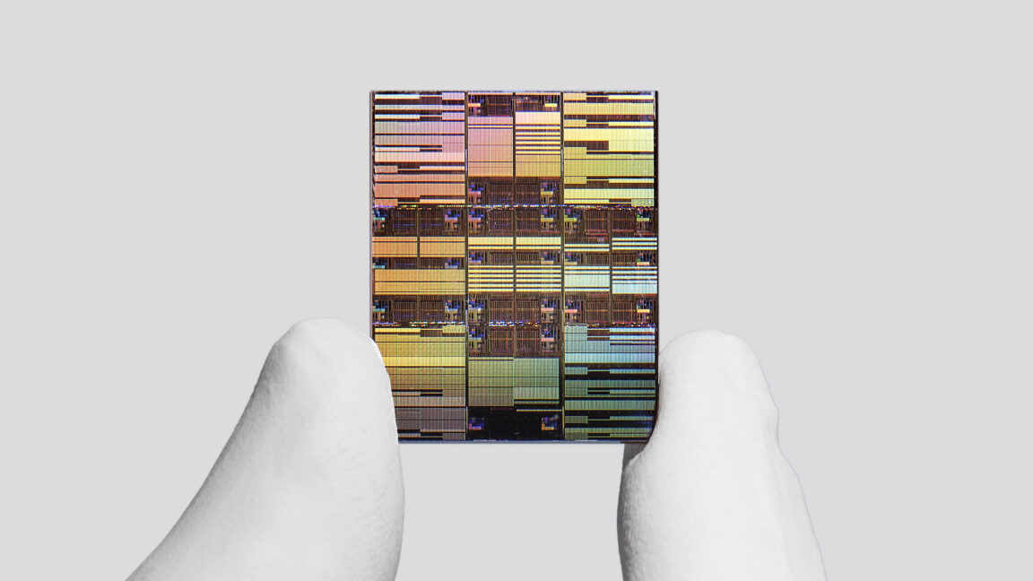
IBM claims world's first sub-1 nanometer chip technology
IBM announced a 0.7-nanometer "nanostack" chip architecture that vertically stacks transistors to deliver performance gains equivalent to sub-1nm scaling.
Deep dive
- The "0.7-nanometer" (7 angstrom) node label refers to performance-equivalent scaling, not the physical dimensions of chip features.
- Architecture utilizes two transistors bonded vertically in a staggered layout.
- Each transistor contains three 5nm-thick nanosheets.
- Enables a 40% improvement in SRAM scaling by reducing the height of the six-transistor bit cell.
- IBM research suggests commercial production in 5 to 10 years, likely through foundry partners.
Decoder
- Nanostack: An architecture where transistors are stacked vertically in a staggered layout to increase integration density.
- Nanosheet transistor: A transistor design where the conductive channel is composed of thin sheets surrounded by a gate on all sides, improving control over current leakage compared to traditional FinFET designs.
- SRAM (Static Random-Access Memory): High-speed, low-latency memory used for CPU/GPU cache, known for being physically large and difficult to scale.
Original article
A new chip architecture from IBM can integrate nearly 100 billion transistors on a chip the size of a human fingernail—nearly twice the transistor density of the company’s previous generation of chip technology. The resulting improvement in chip compute performance and energy efficiency comes from what IBM describes as the “world’s first sub-1 nanometer chip technology” for AI data centers.
“It’s not just an incremental step, it’s a meaningful leap forward,” said Jay Gambetta, director of IBM Research and IBM Fellow, in an advance media briefing. He described the new chip technology as “pointing to a future where computing becomes significantly more powerful without a corresponding increase in energy.”
It’s worth unpacking what the “world’s first sub-1 nanometer chip technology” means, because it is impractical to build reliably functional chips with transistors and other features smaller than 1 nanometer due to various physical limitations. Instead, IBM is basically claiming that its new “nanostack” architecture can deliver the computing performance improvements that would be expected if a theoretical chip could be built with physical features smaller than 1 nanometer.
Specifically, IBM describes its new chip technology as being built at the 0.7-nanometer node, which it has named the 7 angstrom node because 1 nanometer consists of 10 angstroms.
But keep in mind that such node numbers have nothing to do with the actual physical dimensions of IBM’s chip features. Older generations of chips developed in the 1970s and 1980s had physical features with dimensions matching the number in the name of their chip technology’s node or process—such as chips made at the 180-nanometer node—but that has not been the case for decades and certainly not for the latest chip generations made with a 3-nanometer or 2-nanometer process.
To overcome the physical scaling limits facing modern chip designers, IBM’s new nanostack architecture vertically stacks transistors in a staggered layout to pack more transistors into the same chip space. The nanostack architecture builds on the company’s prior development of nanosheet transistors that paved the way for its 2-nanometer chip node introduced in 2021.
The basic unit of IBM’s nanostack architecture consists of two transistors stacked and bonded together. Each transistor consists of three nanosheets that are individually 5 nanometers thick, equivalent to about 15 rows of silicon atoms. There is also a distance of about 9 nanometers separating each nanosheet.
Performance gains for the AI era
The nanostack architecture could pave the way for 50 percent higher computing performance or 70 percent greater energy efficiency than IBM’s previous generation of 2-nanometer node chips, according to projections from the company’s published technical reports. The company introduced its nanostack transistor architecture at the 2025 IEEE Symposium on VLSI Technology and Circuits held in Kyoto, Japan.
IBM researchers also showed how the nanostack architecture can provide 40 percent improvement in scaling for static random-access memory (SRAM) during the VLSI 2026 symposium. SRAM allows for fast but energy-intensive read and write operations that are crucial in many AI applications.
The memory improvement is made possible through a staggered-channel design for the chip’s SRAM bit cells—memory storage units consisting of six transistors—that reduces overall cell height by 40 percent and enables more SRAM to be squeezed into the same chip space.
That will probably be welcome news for chip designers looking to support AI workloads, given how SRAM scaling has fallen off drastically in recent generations of chip technologies. For example, SRAM scaling improved just a few percent between the 3-nanometer chip generation and the 2-nanometer chip generation, Gambetta explained.
“This achievement of 40 percent will eventually industrialize itself in AI workflows, which require higher bandwidth and high efficiency,” Gambetta said.
The roadmap for sub-1 nanometer nodes
As a company that performs chip technology research, IBM does not manufacture commercial chips that could end up in AI data centers or consumer devices. Instead, IBM has partnered with semiconductor companies such as Rapidus in Japan to mass manufacture its previous generation of 2-nanometer node chips based on the nanosheet architecture, or to commercialize related technology in another partnership with Samsung in South Korea.
Other companies have followed up on IBM’s pioneering work without any direct collaboration. For example, Taiwan’s TSMC independently developed nanosheet transistors for its own proprietary 2-nanometer node technology.
“Nanosheet has become the foundation of the next generation of transistor scaling,” said Huiming Bu, vice president of IBM Semiconductors Global R&D and IBM Research, during the media briefing. “Today, nanosheet is adopted by all leading foundries for most of the 3-nanometer chips and all of the 2-nanometer chips.”
IBM declined to name specific companies that it may partner with to commercialize the newest sub-1-nanometer node technology. But Bu expects that commercial chips made at the sub-1-nanometer node and incorporating the newest nanostack architecture could begin production as early as in the next five years and most likely within a decade.
“It will replace nanosheet as today’s mainstream in leading foundries, whether it’s CPUs or GPUs,” Bu said. “Within a decade, this will become another mainstream that we have invented and helped industry to transform.”
Fresh dev news, AI-digested daily. Never miss a trend at devoured.fyi